Background
When I'm experimenting with my 6502 based computer, and using the 6821 Peripheral Interface Adapter (PIA) or the 6522 Versatile Interface Adapter (VIA) I sometimes need to monitor the output ports to confirm data values written to the outputs are correctly presented. Typically I wire up a breadboard with LEDs and resistors, but this can give mixed results especially if any connections are poor quality, incorrectly wired or wires get moved.
I decided to put together a simple display circuit with the aim to produce a Printed Circuit Board where all the components and majority of wiring is static and soldered.
Circuit design
The circuit diagram below allows for the following functions:
1. Monitor up to 8 outputs (from 6821 PIA, 6522 VIA, Raspberry Pi GPIOs, Arduino GPIOs).
2. Monitor 1 to 4 output/inputs (typically 6821/6522 control signals)
3. Paralleled connections to allow additional monitoring using multimeter, oscilloscope, or to drive external circuit(s), or to allow the driving of the PIA/VIA, Raspberry Pi or Arduino.
4. Monitoring LED / resistor combinations to allow use of 5v and 3.3v connections.
5. Paralleled +V and 0V connections.
 |
| 8-Bit-Display Schematic |
Usage
1. Display levels from host circuit GPIO outputs:
Patch o/ps to I/O-1 or I/O-2. Patch I/O-4 pins to 0v. Patch from 0v to the host circuit 0v. When host voltage levels change from 0v to 3.3v or 5v, the corresponding LED will light.
2. Connect +V / 0v levels to host circuit GPIO in input mode.
Multiple +V and 0v patch pins allow for multiple combinations of +V and/or 0v connections to the host circuit. If the host can handle direct +V or 0V connection, I/O-2 could be patched to +V/0V while I/O-1 connects to the host inputs. In this configuration with I/O-4 connected to 0V the LEDs light when I/O-2 goes +V. If the host needs current limiting inputs, the +V voltages can be applied to I/O-3, via resistors to I/O-1 and I/O-2. ALL patching from any LEDs to 0V (I/O-4) must be removed otherwise the LEDs will be damaged.
3. Using the 6821 or 6522, I/O-5 and/or I/O-6 can be used to either monitor or drive the control lines eg. CA1/CA2, CB1/CB2 (some are input only lines). I/O-7 being used to either monitor or patching input voltages/signals.
4. When an external +V voltage is supplied to provide multiple +V, LED (9) lights to act as a reminder/warning of positive voltages on the +V patching pins. C1 provide a decoupling function to help avoid the possibility of any signal noise being present on the +V lines.
5. When using this module to connect to additional host circuits (including such items as the 6821 PIA, 6522 VIA, RaspberryPi, Arduino etc), you must check the data sheets for the items to ensure you don't over supply voltage and/or current to the individual inputs or overload the outputs that could result in excessive current draw from them.
Printed Circuit Board
I've used the PCB design software KiCad, but previous results have been mixed. Looking for some decent instructions, I found a teaching series by Digikey on YouTube.
This series proved invaluable in following the correct steps from circuit design/layout, PCB layout, checking/selecting PCB copper trace(s) sizes, drill hole sizes, solder mask spacing, silk screen production and gerber files creation.
Images below show the unpopulated and fully populated PCBs.
 |
| Unpopulated PCB - Upper Silk-screen side |
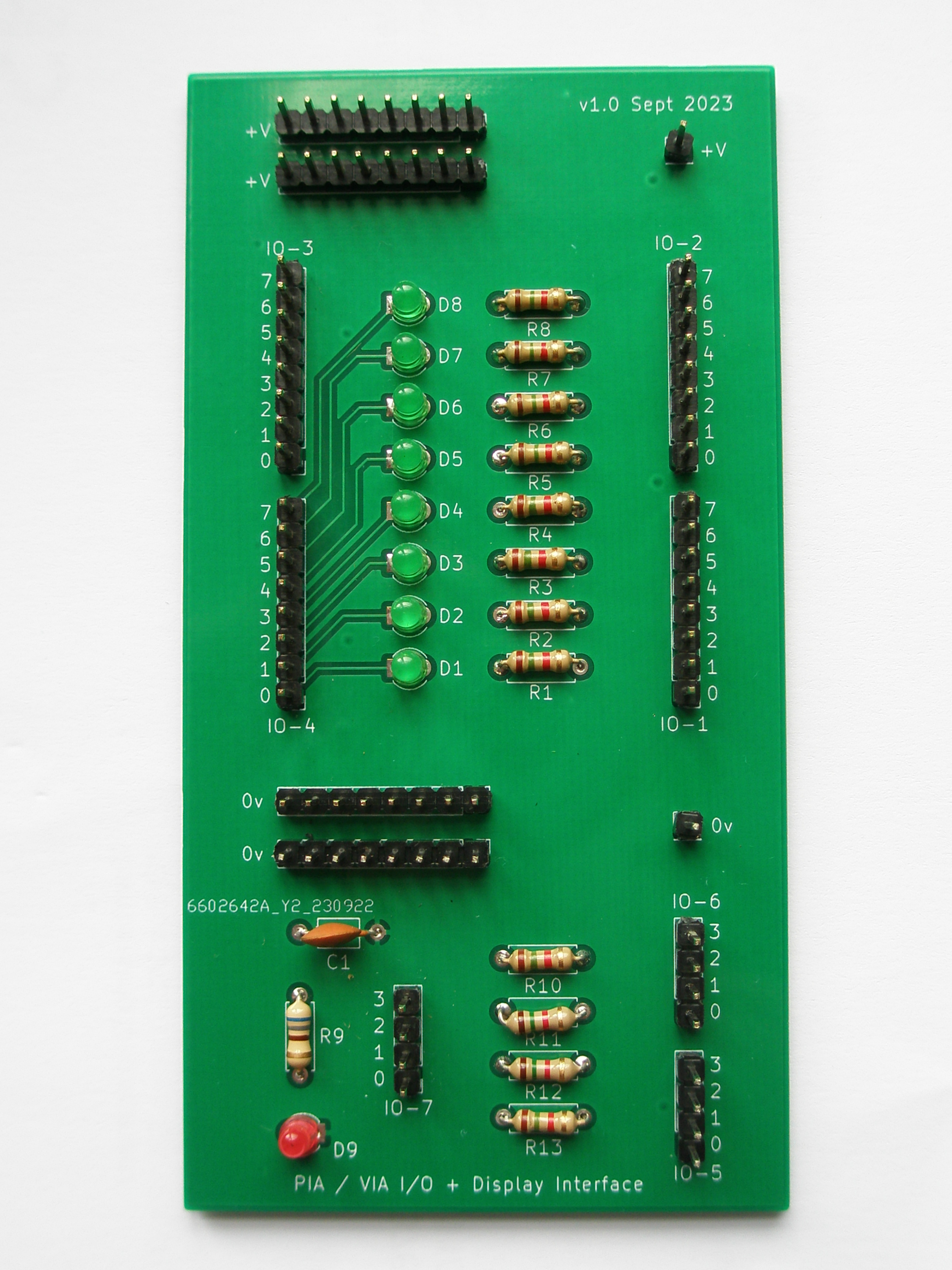 |
| Fully populated PCB |
Having seen the PCB productions from various folk on some technical YouTube channels I decided to use JLCPCB to manufacturer my PCB - a minimum of 5 PCBs per order. The ordering and gerber file uploading process was straight-forward. Tracking of order and production processes proved very interesting, as was the ability to check the delivery status. In all, from ordering to delivery took just 10 working days. The PCBs were just as I had imagined they would look, and very good quality.
Gerber Files
If interested in producing some PCBs, a zipped set of gerber files are available at: (google drive)