Thursday 9 November 2023


Hellorld!

I follow Usagi Electric on YouTube; David set a challenge to create a text string - namely "Hellorld!". As a result of a programming error on his part on a restored Centurion computer, what should have been a "Helloworld!" test message had a few errors.

Following on from this, David has encouraged his followers to recreate this 'error message' on their own computers. Two particular criteria:

1. Must be in assembly or hexadecimal

2. And preferably on a unique machine.

My solution to this challenge involves using a 1-bit computer based on the Motorola MC14500 Industrial Control Unit to generate 7-bit ASCII characters, which connects to my 6502 based computer via a 6821 Peripheral Interface Adapter (PIA). The MC14500 computer also triggers an Interrupt Request on the 6821, to which the 6502 responds with an Interrupt Service Routine (ISR). The ISR reads the data from the 6821, and saves it to the 6551 Asynchronous Communications Interface Adapter, with the ASCII character values sent to a serial display terminal.

The images below show the MC14500 computer (breadboard based), connected to the 6502 computer.

Complete set-up MC14500 & 6502 based computers

The MC14500 1-bit computer

The 6502 based computer

MC14500 Output Register Display - 7-bit ASCII code

The screen shot shows the "Hellorld!" string, repeatedly printed.

'Hellorld!' Serial terminal - displaying ASCII characters from the 6502 computer.
The 6502 hex main code & interrupt service routine code shown above.

MC14500 - 6502 description:

An EEPROM contains the MC14500 instructions - to read an Input Register bit (value = 0), then in turn write out the value or its complement to the Output Register bits 0 to 6 (7 bits in total) to create the ASCII character codes. Bit-7 of the Output Register is written to, to create a single pulse.

Output Register bits 0 to 6 are patched to Port B on the 6821 PIA. The 6821 bit-7 is tied Low as it isn't used and ensures the ASCII code has a leading '0'. MC14500 Output Register bit-7 is patched to the 6821 Control Port (CB1).

The MC14500 cycles through the stored EEPROM instructions, and on reaching the last instruction resets the clock counter, and the routine starts over. The 'speed' of character generation and terminal output can be changed using the MC14500 clock (my circuit runs from 1Hz to 2kHz). It's even possible to use a manual clock - though this takes ages to step through the whole routine.

When the MC14500 writes a 'pulse' to the 6821 PIA CB1, an Interrupt Request from the 6821 triggers an ISR on the 6502.

The 6502 reads the data on the 6821 PIA, writes out the result to a 6551 Asynchronous Communications Interface Adapter (ACIA) to display the characters on a serial terminal at 9600bps (running on my laptop).

Here is a short video showing the MC14500 generation of the ASCII characters, displayed on the serial terminal.


Below I've listed the MC14500 code - fully documented, followed by the 6502 assembler listing. The MC14500 code can be shortened where only single bit changes are made between each change of character. I programmed as below to ensure I was creating the correct values for EEPROM programming. The 6502 code is loaded into RAM, and started from within my 6502 monitor program. The main 6502 code just loops, with the ISR doing the reading/writing of data.

MC14500 listing:

MC14500 coding notes:

8-bit values for the characters Hellorld!

H = 01001000
e = 01100101
l = 01101100
l = 01101100
o = 01101111
r = 01110010
l = 01101100
d = 01100100
! = 00100001
CR= 00001101
LF= 00001010

The binary or hex values are written to/stored in EEPROM

Instruction Code CS Address Binary Hex Note
NOPO 0000 1 000 00001000 08 Flag O 'H'
ORC 0110 1 000 01101000 68 RR goes High, also Data goes High
IEN 1010 1 000 10101000 A8 Input enable
OEN 1011 1 000 10111000 B8 Output enable

Character 'H' = 01001000

LD 0001 1 001 00011001 19 Load value on IR bit-1 > RR [0]
STO 1000 1 000 10001000 88 Store  RR > OR bit-0 [0]
STO 1000 1 001 10001001 89 Store  RR > OR bit-1 [0]
STO 1000 1 010 10001010 8A Store  RR > OR bit-2 [0]
STOC 1001 1 011 10011011 9B Store /RR > OR bit-3 [1]
STO 1000 1 100 10001100 8C Store  RR > OR bit-4 [0]
STO 1000 1 101 10001101 8D Store  RR > OR bit-5 [0]
STOC 1001 1 110 10011110 9E Store /RR > OR bit-6 [1]
STOC 1001 1 111 10011111 9F Store  RR > OR bit-7 [0>1] {strobe pulse}
STO 1000 1 111 10001111 8F Store  RR > OR bit-7 [1>0]

Character 'e' = 01100101

LD 0001 1 001 00011001 19 Load value on IR bit-1 > RR [0]
STOC 1001 1 000 10011000 98 Store /RR > OR bit-0 [1]
STO 1000 1 001 10001001 89 Store  RR > OR bit-1 [0]
STOC 1001 1 010 10011010 9A Store /RR > OR bit-2 [1]
STO 1000 1 011 10001011 8B Store  RR > OR bit-3 [0]
STO 1000 1 100 10001100 8C Store  RR > OR bit-4 [0]
STOC 1001 1 101 10011101 9D Store /RR > OR bit-5 [1]
STOC 1001 1 110 10011110 9E Store /RR > OR bit-6 [1]
STOC 1001 1 111 10011111 9F Store /RR > OR bit-7 [0>1] {strobe pulse}
STO 1000 1 111 10001111 8F Store  RR > OR bit-7 [1>0]

Character 'l' = 01101100

LD 0001 1 001 00011001 19 Load value on IR bit-1 > RR [0]
STO 1000 1 000 10001000 88 Store  RR > OR bit-0 [0]
STO 1000 1 001 10001001 89 Store  RR > OR bit-1 [0]
STOC 1001 1 010 10011010 9A Store /RR > OR bit-2 [1]
STOC 1001 1 011 10011011 9B Store /RR > OR bit-3 [1]
STO 1000 1 100 10001100 8C Store  RR > OR bit-4 [0]
STOC 1001 1 101 10011101 9D Store /RR > OR bit-5 [1]
STOC 1001 1 110 10011110 9E Store /RR > OR bit-6 [1]
STOC 1001 1 111 10011111 9F Store /RR > OR bit-7 [0>1] {strobe pulse}
STO 1000 1 111 10001111 8F Store  RR > OR bit-7 [1>0]

o = 01101111

LD 0001 1 001 00011001 19 Load value on IR bit-1 > RR [0]
STOC 1001 1 000 10011000 98 Store /RR > OR bit-0 [1]
STOC 1001 1 001 10011001 99 Store /RR > OR bit-1 [1]
STOC 1001 1 010 10011010 9A Store /RR > OR bit-2 [1]
STOC 1001 1 011 10011011 9B Store /RR > OR bit-3 [1]
STO 1000 1 100 10001100 8C Store  RR > OR bit-4 [0]
STOC 1001 1 101 10011101 9D Store /RR > OR bit-5 [1]
STOC 1001 1 110 10011110 9E Store /RR > OR bit-6 [1]
STOC 1001 1 111 10011111 9F Store /RR > OR bit-7 [0>1] {strobe pulse}
STO 1000 1 111 10001111 8F Store  RR > OR bit-7 [1>0]

r = 01110010

LD 0001 1 001 00011001 19 Load value on IR bit-1 > RR [0]
STO 1000 1 000 10001000 88 Store  RR > OR bit-0 [0]
STOC 1001 1 001 10011001 99 Store /RR > OR bit-1 [1]
STO 1000 1 010 10001010 8A Store  RR > OR bit-2 [0]
STO 1000 1 011 10001011 8B Store  RR > OR bit-3 [0]
STOC 1001 1 100 10011100 9C Store /RR > OR bit-4 [1]
STOC 1001 1 101 10011101 9D Store /RR > OR bit-5 [1]
STOC 1001 1 110 10011110 9E Store /RR > OR bit-6 [1]
STOC 1001 1 111 10011111 9F Store /RR > OR bit-7 [0>1] {strobe pulse}
STO 1000 1 111 10001111 8F Store  RR > OR bit-7 [1>0]

l = 01101100

LD 0001 1 001 00011001 19 Load value on IR bit-1 > RR [0]
STO 1000 1 000 10001000 88 Store  RR > OR bit-0 [0]
STO 1000 1 001 10001001 89 Store  RR > OR bit-1 [0]
STOC 1001 1 010 10011010 9A Store /RR > OR bit-2 [1]
STOC 1001 1 011 10011011 9B Store /RR > OR bit-3 [1]
STO 1000 1 100 10001100 8C Store  RR > OR bit-4 [0]
STOC 1001 1 101 10011101 9D Store /RR > OR bit-5 [1]
STOC 1001 1 110 10011110 9E Store /RR > OR bit-6 [1]
STOC 1001 1 111 10011111 9F Store /RR > OR bit-7 [0>1] {strobe pulse}
STO 1000 1 111 10001111 8F Store  RR > OR bit-7 [1>0]

d = 01100100

LD 0001 1 001 00011001 19 Load value on IR bit-1 > RR [0]
STO 1000 1 000 10001000 88 Store  RR > OR bit-0 [0]
STO 1000 1 001 10001001 89 Store  RR > OR bit-1 [0]
STOC 1001 1 010 10011010 9A Store /RR > OR bit-2 [1]
STO 1000 1 011 10001011 8B Store  RR > OR bit-3 [0]
STO 1000 1 100 10001100 8C Store  RR > OR bit-4 [0]
STOC 1001 1 101 10011101 9D Store /RR > OR bit-5 [1]
STOC 1001 1 110 10011110 9E Store /RR > OR bit-6 [1]
STOC 1001 1 111 10011111 9F Store /RR > OR bit-7 [0>1] {strobe pulse}
STO 1000 1 111 10001111 8F Store  RR > OR bit-7 [1>0]

! = 00100001

LD 0001 1 001 00011001 19 Load value on IR bit-1 > RR [0]
STOC 1001 1 000 10011000 98 Store /RR > OR bit-0 [1]
STO 1000 1 001 10001001 89 Store  RR > OR bit-1 [0]
STO 1000 1 010 10001010 8A Store  RR > OR bit-2 [0]
STO 1000 1 011 10001011 8B Store  RR > OR bit-3 [0]
STO 1000 1 100 10001100 8C Store  RR > OR bit-4 [0]
STOC 1001 1 101 10011101 9D Store /RR > OR bit-5 [1]
STO 1000 1 110 10001110 8E Store  RR > OR bit-6 [0]
STOC 1001 1 111 10011111 9F Store /RR > OR bit-7 [0>1] {strobe pulse}
STO 1000 1 111 10001111 8F Store  RR > OR bit-7 [1>0]

C/R = 00001101

LD 0001 1 001 00011001 19 Load value on IR bit-1 > RR [0]
STOC 1001 1 000 10011000 98 Store /RR > OR bit-0 [1]
STO 1000 1 001 10001001 89 Store  RR > OR bit-1 [0]
STOC 1001 1 010 10011010 9A Store /RR > OR bit-2 [1]
STOC 1001 1 011 10011011 9B Store /RR > OR bit-3 [1]
STO 1000 1 100 10001100 8C Store  RR > OR bit-4 [0]
STO 1000 1 101 10001101 8D Store  RR > OR bit-5 [0]
STO 1000 1 110 10001110 8E Store  RR > OR bit-6 [0]
STOC 1001 1 111 10011111 9F Store /RR > OR bit-7 [0>1] {strobe pulse}
STO 1000 1 111 10001111 8F Store  RR > OR bit-7 [1>0]

L/F = 00001010
LD 0001 1 001 00011001 19 Load value on IR bit-1 > RR [0]
STO 1000 1 000 10001000 88 Store  RR > OR bit-0 [0]
STOC 1001 1 001 10011001 99 Store /RR > OR bit-1 [1]
STO 1000 1 010 10001010 8A Store  RR > OR bit-2 [0]
STOC 1001 1 011 10011011 9B Store /RR > OR bit-3 [1]
STO 1000 1 100 10001100 8C Store  RR > OR bit-4 [0]
STO 1000 1 101 10001101 8D Store  RR > OR bit-5 [0]
STO 1000 1 110 10001110 8E Store  RR > OR bit-6 [0]
STOC 1001 1 111 10011111 9F Store /RR > OR bit-7 [0>1] {strobe pulse}
STO 1000 1 111 10001111 8F Store  RR > OR bit-7 [1>0]


JMP 1100 1 000 11001000 C8 JMP FLAG goes HIGH > trigger a restart

========================================================================

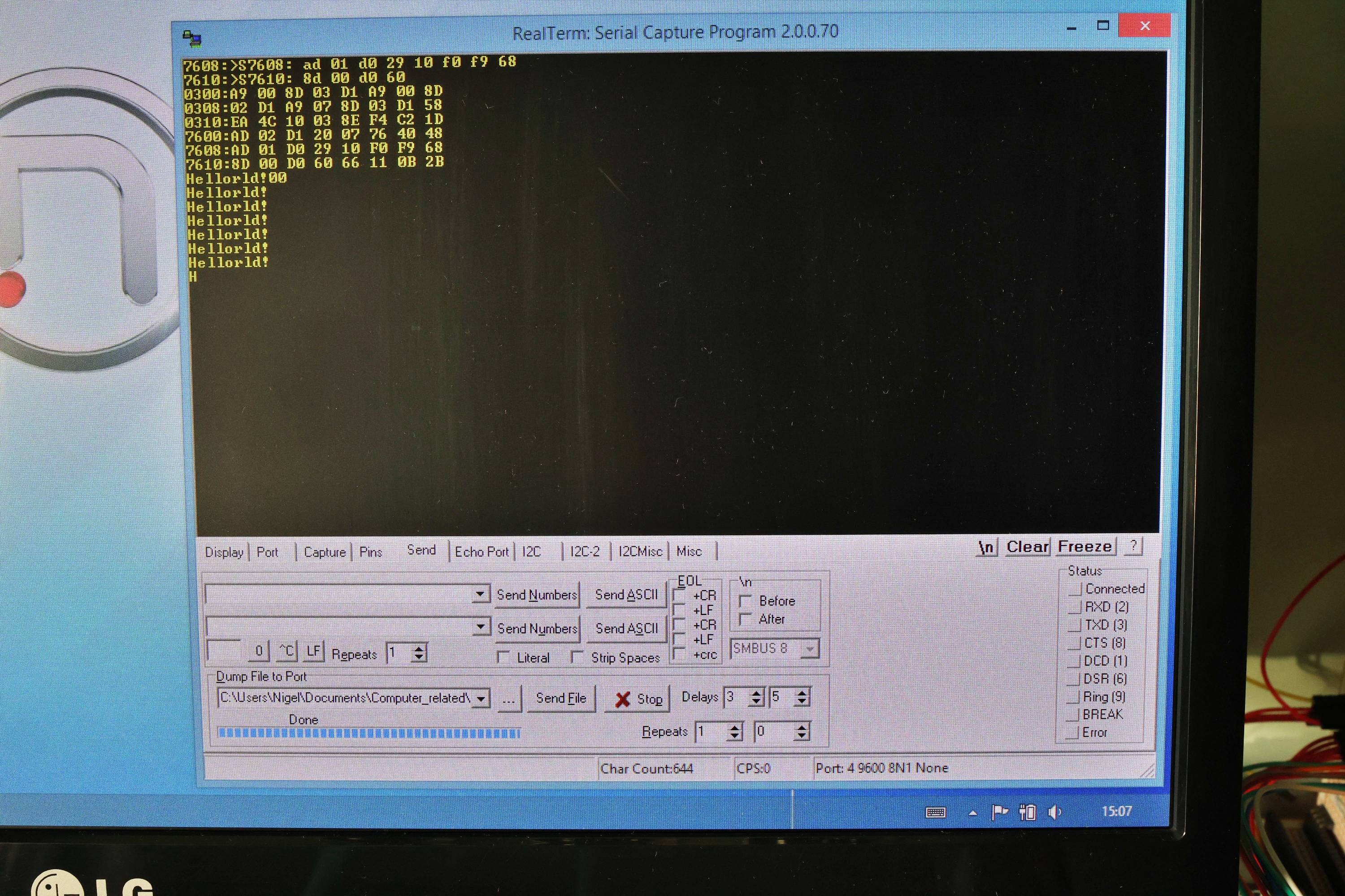
6502 Assembler Listing
; 6502 assembler to configure 6821 PIA, reading input data on an IRQ.
; Send to serial o/p. Run the routine code from within the machine monitor.
; When /IRQ occurs, 6502 reads from the 6821 and writes to the 6551 ACIA.
; The ACIA is already setup as part of the monitor code.
;
; IRQ Vector address $7FFD stored in EEPROM. $7FFD holds a JMP instruction
; to a configurable address (default $7600)
; The ISR start address $7600 is stored in $7FFE ($00) & $7FFF ($76).
; /IRQ Interrupt Service Routine, resides in SRAM - start address $7600.
; Top of SRAM = $7FFF

.target "6502"         ; running a 6502 processor
.code
; Hardware I/O Locations
; ACIA 0
ACIA0_Data = $D000 
ACIA0_Status = $D001 
; PIA-Port-B
PIAB_Data = $D102
PIAB_Control = $D103

; Main code start address
* = $0300

Start
; Configure Port B all Inputs, CB1 /IRQ active, Low to High triggers /IRQ.
; PIA-Port-B
; PIAB_Data = $D102
; PIAB_Control = $D103
;
InitPIAB
LDA #$00 ; Configure the Control Register
; Set bit 0 with '0' this keeps IRQ disabled during setup.
; Set bit 2 with '0' to access DDR on $D102
STA PIAB_Control ; Store in $D103 to access Data Direction Reg. B
;
LDA #$00 ; Configure Data Direction Register - Set bits 0-7 to determine which pins/bits are
                                        ; inputs or outputs
STA PIAB_Data ; Set all bits as inputs ['0' for Input, '1' for Output] store in $D102
;
LDA #$07 ; Configure the Control Register
; Set bit 0 with '1' - enables IRQB set by transition on CB1
; Set bit 1 with '1' - IRQB set by Low to High transition on CB1
; Set bit 2 with '1' - to select Data Register B on $D102 (#$07 = binary 00000111)
; Set bits 3 to 5 with '0' - bit 5 = 0 configures CB2 (not required here)
; (CB1 pin needs connecting to pull-down resistor to avoid false flag on bit-6)
STA PIAB_Control ; store in $d103
; When /IRQB is triggered, connected to /IRQ on 6502, the 6502 triggers 
                                        ; an Interrupt Service Routine
; To read Port B data inputs, PB bits 0 - 7, LDA $D102 // PIAB_Data.
; Reading this clears the IRQ set condition on 6821 IRQB
CLI ; Clear / enable interrupts

Main_Loop
NOP
JMP Main_Loop

; Interrupt Service Routine start address - as set by monitor code.
* = $7600
; The only interrupt request comes from 6821 PIA
; Read Port B - 6821
PORT_READ
LDA PIAB_Data                 ; $D102 - also clears Interrupt Status Flag in Control Register
JSR ACIA0_SendByte                 ; print it
RTI                 ; Return from Interrupt

ACIA0_SendByte                         ; Sends a byte out ACIA 0
                                                        ; Byte must be in A
                                                        ; Returns with registers intact
PHA ; Put A on the stack
A0SB_Loop LDA ACIA0_Status ; Get ACIA Status.
AND #$10 ; Is TX buffer full?
BEQ A0SB_Loop ; Yes. Go ask again.
PLA ; No. Restore A
STA ACIA0_Data ; And send the byte out.
RTS

Thursday 26 October 2023

8-Bit-Display

Background

When I'm experimenting with my 6502 based computer, and using the 6821 Peripheral Interface Adapter (PIA) or the 6522 Versatile Interface Adapter (VIA) I sometimes need to monitor the output ports to confirm data values written to the outputs are correctly presented. Typically I wire up a breadboard with LEDs and resistors, but this can give mixed results especially if any connections are poor quality, incorrectly wired or wires get moved.

I decided to put together a simple display circuit with the aim to produce a Printed Circuit Board where all the components and majority of wiring is static and soldered.

Circuit design

The circuit diagram below allows for the following functions:

1. Monitor up to 8 outputs (from 6821 PIA, 6522 VIA, Raspberry Pi GPIOs, Arduino GPIOs).

2. Monitor 1 to 4 output/inputs (typically 6821/6522 control signals)

3. Paralleled connections to allow additional monitoring using multimeter, oscilloscope, or to drive external circuit(s), or to allow the driving of the PIA/VIA, Raspberry Pi or Arduino.

4. Monitoring LED / resistor combinations to allow use of 5v and 3.3v connections.

5. Paralleled +V and 0V connections.

8-Bit-Display Schematic


Usage

1. Display levels from host circuit GPIO outputs:

Patch o/ps to I/O-1 or I/O-2. Patch I/O-4 pins to 0v. Patch from 0v to the host circuit 0v. When host voltage levels change from 0v to 3.3v or 5v, the corresponding LED will light.

2. Connect +V / 0v levels to host circuit GPIO in input mode.

Multiple +V and 0v patch pins allow for multiple combinations of +V and/or 0v connections to the host circuit. If the host can handle direct +V or 0V connection, I/O-2 could be patched to +V/0V while I/O-1 connects to the host inputs. In this configuration with I/O-4 connected to 0V the LEDs light when I/O-2 goes +V. If the host needs current limiting inputs, the +V voltages can be applied to I/O-3, via resistors to I/O-1 and I/O-2. ALL patching from any LEDs to 0V (I/O-4) must be removed otherwise the LEDs will be damaged.

3. Using the 6821 or 6522, I/O-5 and/or I/O-6 can be used to either monitor or drive the control lines eg. CA1/CA2, CB1/CB2 (some are input only lines). I/O-7 being used to either monitor or patching input voltages/signals.

4. When an external +V voltage is supplied to provide multiple +V, LED (9) lights to act as a reminder/warning of positive voltages on the +V patching pins. C1 provide a decoupling function to help avoid the possibility of any signal noise being present on the +V lines.

5. When using this module to connect to additional host circuits (including such items as the 6821 PIA, 6522 VIA, RaspberryPi, Arduino etc), you must check the data sheets for the items to ensure you don't over supply voltage and/or current to the individual inputs or overload the outputs that could result in excessive current draw from them.

Printed Circuit Board

I've used the PCB design software KiCad, but previous results have been mixed. Looking for some decent instructions, I found a teaching series by Digikey on YouTube.

This series proved invaluable in following the correct steps from circuit design/layout, PCB layout, checking/selecting PCB copper trace(s) sizes, drill hole sizes, solder mask spacing, silk screen production and gerber files creation.

Images below show the unpopulated and fully populated PCBs.

Unpopulated PCB - Upper Silk-screen side

Fully populated PCB

Having seen the PCB productions from various folk on some technical YouTube channels I decided to use JLCPCB to manufacturer my PCB - a minimum of 5 PCBs per order. The ordering and gerber file uploading process was straight-forward. Tracking of order and production processes proved very interesting, as was the ability to check the delivery status. In all, from ordering to delivery took just 10 working days. The PCBs were just as I had imagined they would look, and very good quality.

Gerber Files

If interested in producing some PCBs, a zipped set of gerber files are available at: (google drive

Saturday 25 July 2020

6522 Shift Register - Shift in under PH02 clock

Introduction

6522 Shift Register - Shift in under PH02 clock

In this article I share my findings in the configuration and use of the Shift Register in Mode 2. The approach to this, the code and methods used may appear convoluted, but I have learned so much in the process.  [6522 configuration and usage, 74165 and 7474 usage, Arduino interrupt programming].

Hopefully you will find some of this article interesting and maybe even useful.


SR Mode 2 - Shift Serial Data in under control of PH02

The shift rate is a direct function of the system clock frequency.

CB1 becomes an output which generates shift pulses for controlling external devices.

The shifting operation is triggered by either reading from or writing to the Shift Register.

Data is shifted, first into bit 0 and is then shifted into the next higher order bit of the shift register on the trailing edge of each PH02 clock pulse.

After 8 clock pulses, the shift register interrupt flag (IFR) will be set, and the output clock pulses on CB1 will stop. At this point the data is held in the Shift Register. Another read of the Shift Register is needed to retrieve the data to the CPU. Doing this read clears bit 2 of the IFR, and generates another 'shift-in' sequence, after which, bit 2 IFR is set again.


The challenge

Having work through the majority of the 6522 operating modes, the 'shift serial data in' mode posed its own challenge to me. Generating outputs from the 6522 can be monitored on an oscilloscope, or by using LEDs connected to the various ports. Generating parallel input data on Port A or B can be achieved manually. Getting the 6522 to generate a shift-in clock together with generating a 'trigger pulse' for an external device to respond with providing serial data to the 6522 was quite a challenge.


The experiment

Part of the experiment uses the idea put forward by Garth Wilson at:

http://wilsonminesco.com/6502primer/potpourri.html#22_SR_INnOUT

This uses a 74165 (parallel to serial shift register), to provide serial data and a 7474 (Dual D-Type Positive Edge Triggered Flip-Flops). Garth helpfully describes the rationale for using the 7474 to delay the data to ensure the data is shifted from the 74165 to the 6522 correctly.

The first experiment I tried was to manually configure the 74165 and wrote a short piece of code to read one byte into the 6522 Shift Register. This worked well and as expected.

The second experiment I tried was to use an Arduino board to generate 8-bit parallel data, connected to the 74165. The Arduino was used in an interrupt mode, triggered by a low pulse from the 6522, to generate an 8-bit byte to load into the 74165. After this operation, the 6522 is used to shift in the data and store the data in memory, and write out to LEDs connected to Port A.


The Block diagram:


The circuit diagram:

For clarity, the circuit diagram omits connections to power and many connections associated with the 6522 VIA and the Arduino.


The 6502 assembly code notes & process flow:

6522

CB1 used to generate the clock signal (8-bits)

CB2 used as the serial shift input from the 74165 shift register

CA2 used to enable the 74165 for loading data, and to trigger the Arduino to load the 74165 with 8-bit parallel data (by taking CA2 -ve).

CA2 defaults to HIGH, enabling the 74165 output mode.

Registers used:

ACR - Auxillary Control Register, write $08 Mode 2 =  Shift in under PH02 control

IFR- Interrupt Control Register, write $7F, Clear

IER - Interrupt Enable Register, write $84,  Set Shift Register IRQ

SR - Shift Register, read SR, generates shift clock on CB1, reads in data on CB2

PCR - Peripheral Control Register, write $0A, sets 'Pulse Output' mode - CA2 normally High

DDRA - Data Direction Register A, write $FF, set Port A as outputs

IRA - Input/Output Register A,  write $xx, sets data on Port A


Process flow

* Set up DDRA, IFR, IER, ACR, PCR

* Use the PCR to generate -ve pulse on CA2, enables the 74165 for loading, 'triggers' the Arduino to output data to the 74165 (loads the data into 74165)

* CA2 returning High enables serial o/p from 74165

* Write $00 to the 6522 SR, clears the SR and an 8-bit clock stream is generated on CB1, when complete the IFR bit 2 is set, the /IRQ line goes Low. The clock stream, applied to the 74165, clocks the parallel data on the 74165 to the 6522 Shift Register.

* To get the data from the SR to the CPU, read the SR. This resets the IFR and /IRQ goes High. Reading the SR also generates another 8 clock pulses. When complete, the IFR is set and /IRQ goes Low.

* A clear of the IFR is needed, this also sets /IRQ High.

* Store the read data value in memory and write data to port A outputs.

* Return to monitor [monitor re-entry address = $E070]


Oscilloscope traces:


Top trace: CA2 line drops -ve to trigger Arduino and enable 74165 for loading

Middle trace: Arduino bit-7 indicates when the Arduino data byte is complete for 74165 loading

Lower trace: CB1 Shift Clock pulses from 6522


Top trace: CA2 - after 74165 data loaded, CA2 returns High to allow 74165 serial output

Middle trace: CB1 Shift Clock pulses from 6522

Lower trace: CB2 Serial data from 74165/7474 to 6522 Shift Register In (data value $FA).

The second set of 8 clock pulses is the 6522 response from executing a read of the 6522 SR.


Zoomed in copy of previous display:

Top trace: CA2 - after 74165 data loaded, CA2 returns High to allow 74165 serial output

Middle trace: CB1 Shift Clock pulses from 6522

Lower trace: CB2 Serial data from 74165/7474 to 6522 Shift Register In (data value $FA).


6502 Serial Terminal Screen display (using 'screen' on RaspberryPi)

Running the 6502 code at $1000 runs through the 6502 code below once. Running this routine 4 times shifts in the 3 data byte values held by the Arduino ($FA, $FB and $FC). These values are stored in zeropage RAM at address $0016. The values are overwritten each time the 6502 routine is run.


Conclusions:

This experiment (for me) was quite challenging, and I learned so much doing the research, writing the 6502 and Arduino code and interpreting the oscilloscope displays to work out the various signal timings to ensure all the different elements worked together. Although unlikely to be a useable and practical way of getting data into the 6502 RAM, I envisage that with minor modification it would be possible to load large quantities of data from the Arduino to the 6502 computer.

The 6502 assembly code:

.target "6502"
.code
* = $1000
         ; zeropage locations
inb =  $0016  ; holds byte value received
         ; 6522 VIA settings
IRA = $D201  ; address of Input Port A
DDRA = $D203  ; data direction register for Port A
ACR = $D20B   ; Auxillary Ctrl Reg
IFR = $D20D  ; Interrupt Ctrl Reg
IER = $D20E  ; Inteerupt Enable Reg
T2 = $D208  ; T2 Low Timer/Counter [only needed if using T2 control]
SR = $D20A  ; Shift Register
PCR = $D20C  ; Peripheral Ctrl Reg
initvia:
lda #%11111111 ;
sta DDRA         ; set VIA Port A all outputs
sta IFR ; Clear IFR
lda #%10000100 ; enable Shift Register IRQ
sta IER ;
lda #%00001000 ; $08
sta ACR ; Shift In under PH02 Clock Ctrl
lda #%00001110 ; set CA2 high default
sta PCR ; sets SH line High, 74165 ready to shift

entry:
lda #%00001100 ; set CA2 Low
sta PCR ; a low on CA2 connected to the /LD on the 74165 and
                                        ; the Arduino UNO [falling IRQ] will trigger an ISR on 
                                        ; the UNO to send 8-bit byte parallel data to the 
                                        ; attached 74165
                                        ; a delay is needed of approx 40uSecs between setting
                                        ; CA2 LOW and returning it HIGH to allow time for the
                                        ; Arduino to load the data
                                        ; delay here
ldx #$F0         ; initialize xreg, $F0 = delay ~ 102uS
                                        ; [more than needed]
delay:
inx         ; increment
bne delay         ; loop if not zero
lda #%00001110 ; set CA2 high
sta PCR ; return SH/LD line High, 74165 ready to shift
lda #$00         ;
sta SR ; clear SR, this initiates clock pulses (x8)
loop1:
lda IFR ; check Interrupt Flag Register
and #$04         ; has the SR completed 8 shifts?
beq loop1         ; no, keep checking
        ; yes, IFR bit 2 set [and = 1]
        ; serial data read in to the SR on CB2, /IRQ = Low
lda SR ; read the SR, transfers data to the CPU
        ; IFR bit 2 is cleared, another 'shift-in' sequence occurs
        ; and sets IFR & /IRQ when sequence ends
nop         ; allow time for read & sequence to end
nop         ; otherwise the clear IFR /IRQ (below) is missed
nop         ;
sta inb ; store data byte received to zeropage store
sta IRA ; store byte value to port A LEDs
        ; using the PCR to control CA2 directly means that
                                        ; writing to IRA doesn't generate a -ve pulse on CA2,
                                        ; avoiding loading data to 74165
lda #%11111111 ; $FF
sta IFR ; Clear IFR (clear the interrupt condition/flag)
nomore:
jmp $E070 ; Go back to the monitor.


 Arduino UNO code:

// Interrupt routine
// Normal operation is just a void loop
// -ve pulse generated and applied to pin D2 - the CA2 line on the 6502
// interrupt occurs when -ve 'falling' level detected
// Interrupt Service Routine (ISR) is executed and when completed,
// returns control to the 'loop'
// On the Arduino UNO, pins 2 and 3 are capable of generating interrupts
// and they correspond to interrupt vectors 0 and 1 respectively.

const int pulsePin = 2; // -ve pulse here (6502 CA2 line)
int count = 0;         // data read count from array counter

// UNO data pins (5 to 12) connected to 74165 parallel data input pins
#define DATA_D0 5
#define DATA_D7 12

// put data here to 'shift' into attached 74165 shift register
byte digitsHEX[] = {0xFA, 0xFB, 0xFC};

void setup() {
 // pulse pin as an input
 pinMode(pulsePin, INPUT);
 // configure 8 data pins as o/ps
 for (int pin = DATA_D0; pin <= DATA_D7; pin +=1){
    pinMode(pin, OUTPUT);
 }
 // attach interrupt to the ISR vector
 attachInterrupt(digitalPinToInterrupt(pulsePin), pin_ISR1, FALLING);
}

void loop() {
  // nothing happening
}

void pin_ISR1(){
  // Interrupt Service Routine - get data from array, 
  // write single 8-bit byte value out
  writeData(digitsHEX[count]);
  count +=1;
  // test to ensure data array read doesn't go out of range
  if (count > 2) {
    count = 0;
  }
}

void writeData(byte data){
  // write out 8-bit data from array on digital pins 5 to 12 
  for (int pin = DATA_D0; pin <= DATA_D7; pin +=1){
    digitalWrite(pin, data & 1);
    data = data >> 1;
  }
}